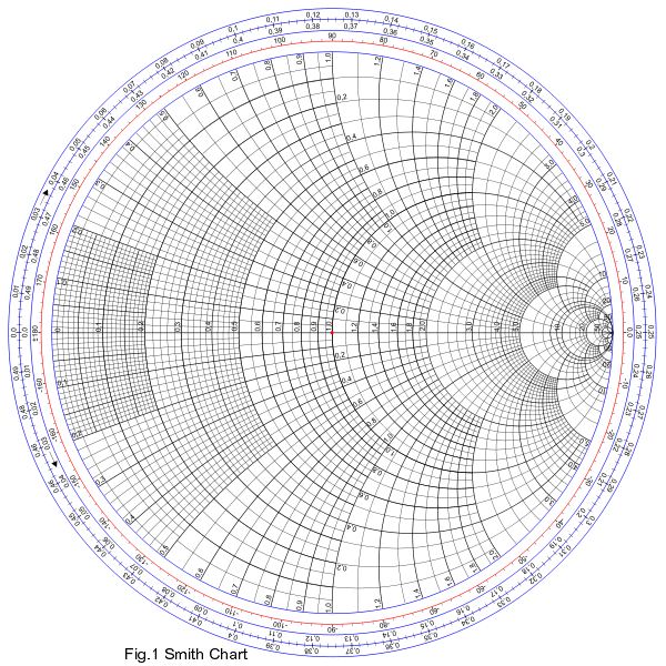
Its wonderful to see the progress made by the III-V technology companies in providing the foundry services and products for really high performance products and MMICs. When I started in GaAs the maximum wafer size for a GaAs wafer was about the size of my thumbnail. Today there are Si-GaAs wafers 12 inches across! Design tools for simulation and characterization have also come a long way. Before these developments we were designing MICs and there were none or very few design tools. We matched the input and out reflection coefficients using tiny gold disks of various radii to achieve the optimum matching. I remember getting 1 Watt out of a GaAs FET. It was unknown during those days. It took a thermal bonder, much sweat ( and tears) and precise bondwire matching and the rest of the work to achieve this. Today I work with ADS and similar tools to seriously reduce risk before layout and post layout of the MMICs. MMIC packages have come a long way too. During the days I was learning MMIC design, no packages were available. The die was mounted directly on the Alumina substrate. Now we can get touchstone files for packages and along with the s – parameters of the device itself, a reasonable match can be done a priori. Devices such as pHEMTs were not available then. They are available now. By the way we used TWT’s to test the devices. These were the test boxes provided by HP to test those high frequencies ( mostly X Band) we were designing in. So with the foundry services, the CAD tools, the package data and test equipment available today, MMIC development is much less of a risk today than it used to be. Good job and kudos to all the companies who have made it possible. By the way the accompanying image of the Smith Chart is a reflection ( no pun intended) of the workhorse tool of those early days of MMIC design. By Ain Rehman, Signal Processing Group Inc.


