Analog and RF/Wireless integrated circuit and module design professional with over 38 years of experience in the industry. Worked for Fortune 500 companies for 18 years (Intel, ITT, Plessey and GTE. Currently employed by Signal Processing Group Inc.
GM-C filters can be very useful when designing in fine line MOS or in a CMOS or BiCMOS technology. The capacitor sizes can be made small and thus save chip area. They can be easier to test. If the prototype filter is designed with lumped L and C components then these can be replaced with solid state blocks such as integrators. GM – C theory is fairly well understood so the risk in design is relatively low. SPG presents a report on a GM-C bandpass filter we did for interested readers ( engineers, students and Instructors) with an earnest hope that it will be useful. Please visit the SPG website and read or download the report.
Calculating the resistor parameters ( length, width resistance etc.) is a common task done by IC designers when a chip is designed. This post introduces a simple Javascript calculator that calculates the length of a resistor, given the sheet resistance of the technology, the required resistance and the width of the design rule for resistors. This calculator provides a starting point quickly to do the calculation. It is the first order value of the resistance. Please download the calculator from the SPG website to use it.
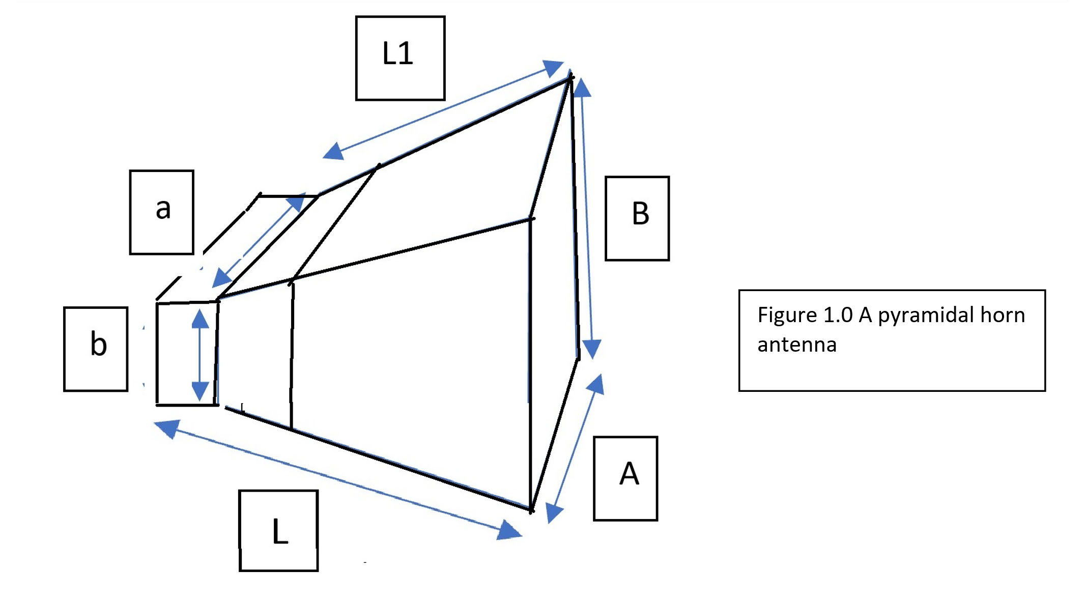
This post describes a methodology for the design
of a pyramidal horn antenna. Following posts build on it and provide more
details. A pyramidal horn is a popular antenna that has very little loss and is
used commonly in antenna systems. The
structure of the pyramidal horn is shown in FIGURE 1.0 below.
Pyramidal horn structure
The design of a horn like this begins with a
specification. Usually the following parameters are given:
Gain (in dBi)
a (inches or cm) (usually the horn is fed from a waveguide)
b (inches or cm) (usually the horn is fed from a waveguide)
frequency (Hz)
The problem is to find A and B, and other dimensions shown below. Once we
have these dimensions, we can find other parameters of the antenna.
The usual procedure is to solve an equation to get a key parameter
using the given specifications. This methodology will be outlined in this post
and access to the equation solver will be provided. Subsequent posts will add
more detail so that an engineer will be able to get a first cut design of the
horn and fabricate it.
After the required key value is obtained through
solving the equation the following steps are used to find the Horn parameters.
Use
λ is the wavelength of the signal in cm. le is found from the
solution of the equation.
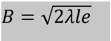
Calculate B from this equation.
From B, λ, le and G calculate A. The
equation to be used is:
G = (½)(4π/λ2)(AB)
Now we have A and B.
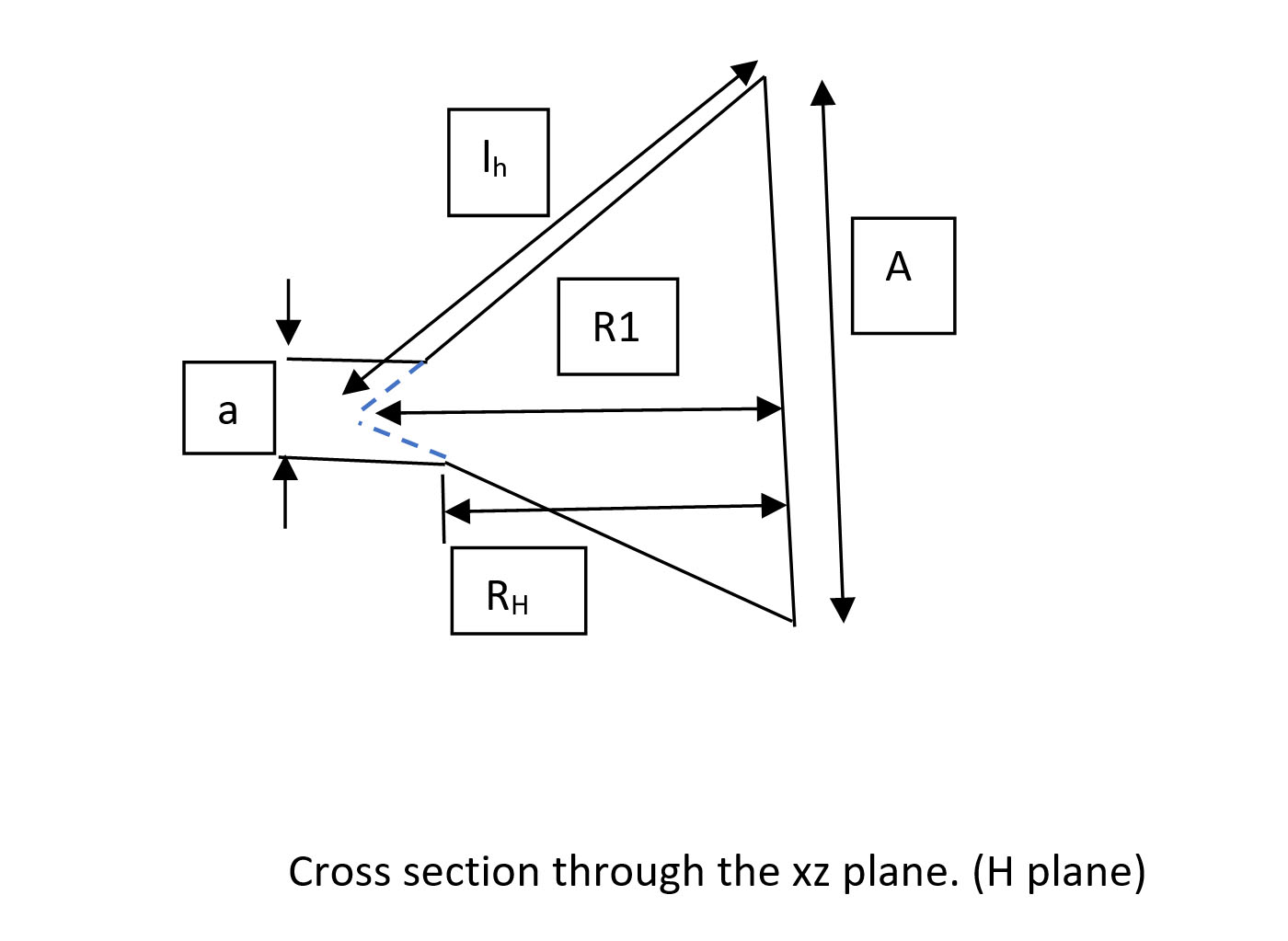
lh is found from the following equation:
A = sqrt(3λlh)
Calculate RH and RE from the following equation:
RE = (B -b)(sqrt[(le/B)2 – ¼)])
Since we are dealing with a pyramidal horn RE =RH
Use the following equation for R1:
lh2 = R12 + (A/2)2
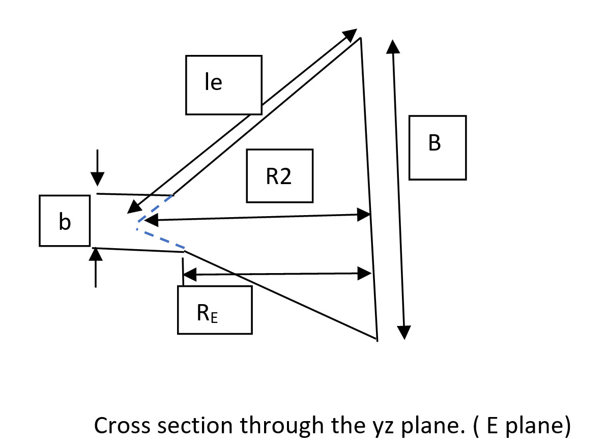
Use the following equation to calculate R2:
le2 =
R22 + (B/2)2
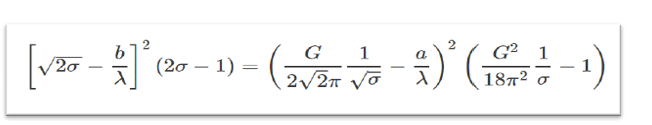
The equation to be solved is:
The quantity σ has to be solved for. σ =le/λ . This equation is best solved numerically with a starting value of σ = G/2π√6. The Python program that was written to do this is available on request at spg@signalpro.biz or spg327@gmail.com
Ref: This blog is partially based on “Antenna Theory and Design, by Warren L. Stutzman and Gary A. Thiele. The book was published by John Wiley and Sons, 1981. Ref: The Python program was written by Anuj Tripathi, University of Arizona, Tucson, Arizona.
Recently we published a calculator that provides the value of an inductor wound on a toroid given the number of turns of wire and other parameters.
A reverse calculator is provided now by SPG that calculates the number of turns needed to generate a given value of an inductor wound on a toroid. Please visit the SPG website and check under the “complementary” menu.
The inductance of a toroidal inductor can be calculated using the following simple expression: L = AL*n*n/1000 uH. AL is a constant provided by the manufacturer of the toroid and n is the number of turns of wire.. Please visit the SPG website for more technical articles and items of interest.
A simple Javascript calculator for resistance of semiconductor layers.
The resistance of a resistive layer on an ASIC/IC is usually given (for hand calculations ) by taking the ratio of the length of the layer and its width and multiplying by its sheet resistance, (L/W)RS. Where L is the length, W is the width and RS is the sheet resistance. (Not every resistor can be calculated this way. Odd shapes are not amenable to this formula.) A simple javascript was generated at SPG that can be modified as needed to do this. Please visit the Signal Processing Group website to download the calculator free of cost. The calculator may be found under the “calculators” menu item.
A recent post presented the Colpitt’s oscillator starting point with a schematic and simulation results. In addition, it also provided a link to the recent book by Ain Rehman on this oscillator available from Amazon that contains design information and an exhaustive list of references for further study for interested readers. This post suggests downloading the Colpitt’s oscillator frequency calculator from the SPG website. It provides a good starting point and sanity check on the design of a Colpitt’s oscillator for the user. Please visit the SPG website and look under the ” Complementary” menu item.
3D design and printing has been gaining momentum recently for use in various applications — from microstructures to houses. Electronic enclosures and other parts are no exception. 3D design and printing is a quick way to make enclosures and fast prototypes using many different types of materials. The image below is a lighthearted print of a dragon. Be that as it may, if you want to print using a 3D printer please contact us for a bid as well. Please visit the SPG website for more information on our capabilities in electronics, ASICs and RF/Microwave modules.
A new book on the subject of the Colpitt’s Oscillator was just released on Amazon. This is a small book (text wise) but with an extended coverage of the subject for hands on work by engineers and students and other interested readers. It is very economical as far as the text and mathematical derivations go but supported by javascripts and a very extensive list of references that causes the virtual footprint of the book to be fairly massive. Interested readers may pick it up from Colpitt’s Oscillator: Theory, design, simulation, references: Rehman, Mr Ain: 9798406680810: Amazon.com: Books