Small loop antennas: Resistances and efficiency

The radiation resistance of a small loop is given by: 3.12*10**4[NA/(lambda*lambda)]. Here N is the number of turns, A is the area of the loop in square meters, lambda is the wavelength of operation in meters. The radiation resistance of a small loop is very low. The loop also has losses. So an efficiency can be calculated as: ETA = Rrad/(Rrad+RL). Here RL is the loss resistance. ETA can be expressed as a percentage also. Note that RL is the loss in the conductor and the loss in the series tuning capacitor that is frequently used. The effect of the ratio of Rrad/RL can be derived. Some common points of reference are: Rrad/RL = 100. ETA = 100%, Rrad/RL = 0.01, ETA = 0.0 ( approximate), Rrad/RL = 1.0, ETA = 50%.For further information please search for small loop antennas in this blog to access the EXCEL spreadsheet useful in designing a practical antenna or visit http://www.signalpro.biz and look under ” free stuff”..

We design and deliver analog and RF/wireless ASICs and modules using state of the art semiconductor, PCB and assembly technologies. Please contact us at spg@signalpro.biz for a quote and a proposal.


Small loop antennas: Interesting information

Small loop antennas are very useful structures used extensively in the radio world. However, the question is: what exactly is a small loop antenna? By definition a loop antenna is considered small when its total conductor length is less than 0.1 – 0.085 of the wavelength. This definition is based on the fact that the current around the perimeter of the loop must be in phase. When the winding conductor is more that 0.085 of a wavelength long, this is no longer true. The simplest loop antenna is a single turn of a conductor loaded at a pair of its terminals at the center of one of the sides. A good tool to use to understand and analyze this structure is the freeware program NEC2. The voltage generated across the terminals of the loop is given by a simple expression: V=[2.0*pi*A*N*E*Cos(theta)]/lambda. lambda is the wavelength of operation, pi=22/7, A is the area of the loop in square meters, N is the number of turns in the loop, E is the RF field strength in volts per meter, theta is angle between the plane of the loop and the signal source ( transmitter). For further information please search for small loop antennas in this blog to access the EXCEL spreadsheet useful in designing a practical antenna or visit http://www.signalpro.biz and look under ” free stuff”..( More to come on small loops)

We design and deliver analog and RF/wireless ASICs and modules using state of the art semiconductor, PCB and assembly technologies. Please contact us at spg@signalpro.biz for a quote and a proposal.

A high frequency FM modulator ( VCO) module from SPG

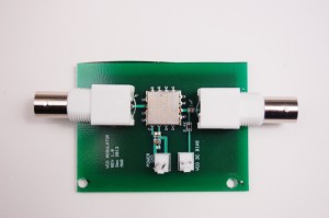
A standalone VCO can be a valuable tool in test and design efforts. Recently Signal Processing Group Inc.,designed and released a fully assembled VCO/FM Modulator module running up to 1624 Mhz. The supply voltage is 5.0V, the I/O consists of BNC connectors. The Output impedance is 50 Ohm. The center frequency ( or rest frequency) can be set by a DC input. The modulating frequency is connected through a BNC connector.( See the image below). Further details can be obtained by contacting us on (email) spg@signalpro.biz. Other frequency ranges are available and a custom module can be acquired at no additional cost. Again please contact SPG for further details.

A standalone VCO/Frequency modulator module


We design and deliver analog and RF/wireless ASICs and modules using state of the art semiconductor, PCB and assembly technologies. Please contact us at spg@signalpro.biz for a quote and a proposal.

A wideband rf amplifier module from SPG

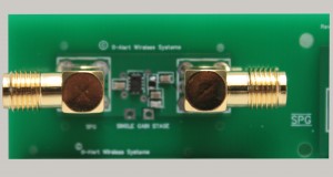
A RF amplifier module designed and assembled by Signal Processing Group Inc. has been released for acquisition by interested parties. This module consists of a wideband (> 1Ghz ) amplifier chip with its supporting external components and SMA I/O. It can be used for multiple purposes from test to design of more complex systems. The gain is 20 dB, with 50 Ohm input and output impedances. Obviously a number of these modules can be cascaded to provide higher gains in mulltiples of 20  dB. The power supply is 3.3V. Further details are available from SPG by contacting us through our website located at http://www.signalpro.biz or by directly contacting us on ( email) spg@signalpro.biz.

A wideband RF amplifier, available for purchase from Signal Processing Group Inc.

A wideband RF amplifier

We design and deliver analog and RF/wireless ASICs and modules using state of the art semiconductor, PCB and assembly technologies. Please contact us at spg@signalpro.biz for a quote and a proposal.

Surface mount passive component value marking

Surface mount components ( resistors, capacitors, inductors) are harder to identify than their through – hole counterparts.. In addition they are very small ( the smallest in practical use is the 0402 size ( 40 mils by 20 mils). Almost impossible to see with the naked eye. If you find a SMD component what are its markings indicating? Here is some information about this which may be useful ( specially if you do a lot of surface mount assembly by hand). (1) Resistors: These will have either 3 or four digits on them. The last digit is simply the number of zeros after the first few digits. For example 473 is 47 followed by three zeros or 47k. Another example is 5673. Same old rule. This is a 567k resistor

(2) Capacitors are more difficult: Sometimes there may not even be any labeling If there is labeling, it is the same as SMD resistors, but in pF. Polarized capacitors have a stripe on the positive end of the package. Some electrolytic SMT capacitors may be marked on the negative end of the package. They are rectangular, and often black or tan colored. The black capacitors can be easily mistaken for diodes because of the white stripe on one end.

(3) Inductors: An inductor may use the color code system. If so the value represented is in µH. There may be a wide silver or gold band before the normal colored bands. A thin tolerance band at the end may also be there.

Modeling the Sigma – Delta modulator using PSPICE

A sigma – delta modulator is used in a variety of applications. One application is that of a A/D converter. In order to understand the operation in a intuitive way ( and the sigma -delta A/D is not a circuit open to intuitive understanding), a behavioral model can be very, very helpful. Recently a first order sigma – delta modulator was modeled and its operation was understood. Interested parties can contact us at the website located at http://www,signalpro.biz. A complete PSPICE behavioral model is available for experimentation.

We design and deliver analog and RF/wireless ASICs and modules using state of the art semiconductor, PCB and assembly technologies. Please contact us at spg@signalpro.biz for a quote and a proposal.